Semiconductor Materials
Demand for higher product quality is increasing as semiconductor devices and electronic components become progressively smaller and more integrated. At Shin-Etsu Polymer, all manufacturing processes for wafer containers are handled in clean rooms to minimize the possibility of particle contamination in the materials of the containers, which are used in front-end processing of semiconductor devices.
We also make proposals involving “Shin-Etsu Lightframe” and package inspection MT-type inter-connectors for enhancing the reliability of the back-end package assembly process.
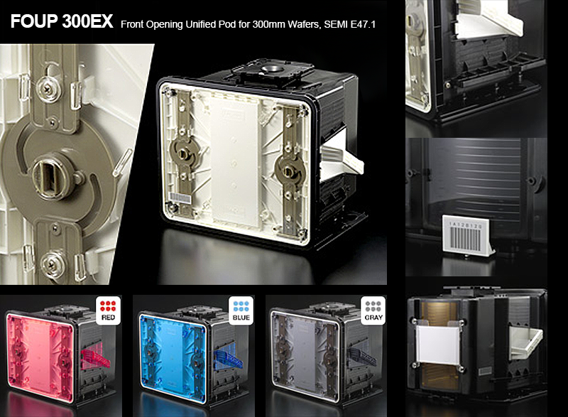
Wafer Cases
Shin-Etsu Polymer has two kinds of front opening shipping boxes (FOSBs) used for transporting wafers between wafer and device manufacturers. We also make front opening unified pods (FOUPs) for device makers’ manufacturing processes. Shin-Etsu Polymer’s FOSBs and FOUPs are known for their high quality and reliability in the global semiconductor industry. Click product detail below.
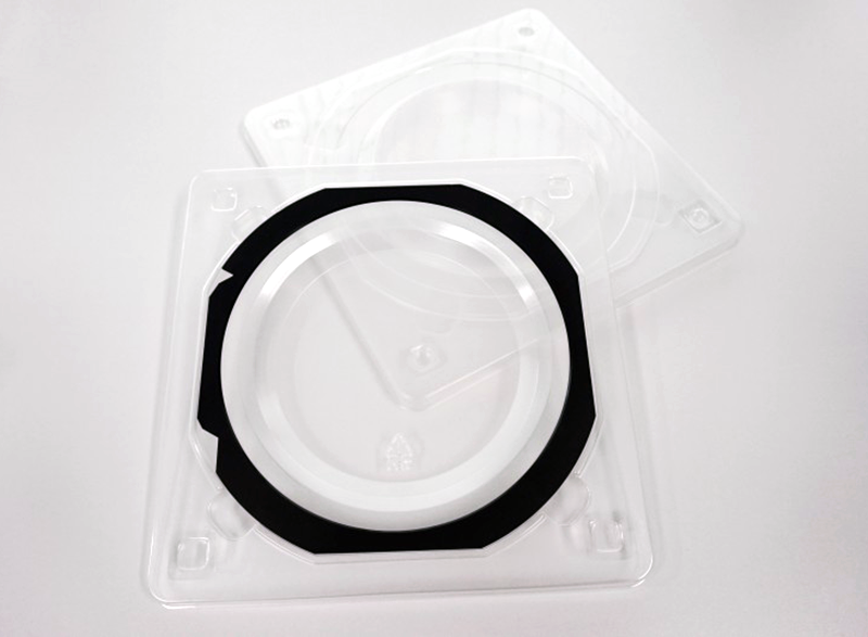
Plastic Tape Frame
Shin-Etsu Lightframe® reduces conductive particles by using metal tape frame and improves the reliability for packages. Characteristics: Conductive particles reduction, Light weight, Ease of operation, Suitable for RF-ID tags, Conformance to SEMI Standard (300 mm dia, conforming to SEMI G87-1108)
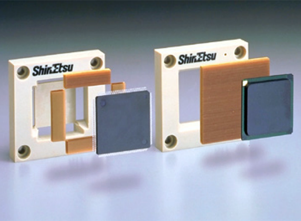
Inspection of Semiconductor/Electrical Devices
Applied for inspection of semiconductor and high frequency devices. MT series has short conductive route, therefore, is superior in high frequency transmission. The life time is much longer than the other types. Used for extensive applications including CPU or high frequency filter inspection.


